Reference · Generations
The Link Speed Table
One table, one row per generation, and a column that says where the figure came from. Everything else on this site refers back to it.
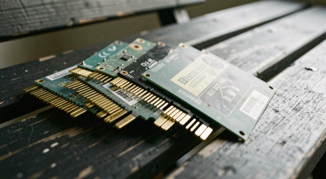
What a rate row contains before any generation label
Every speed claim about a PCI Express link compresses three numbers into one, and the compression is where the errors enter. The first number is the raw transfer rate, counted in gigatransfers per second, GT/s: how many bit times the wire clocks out, whatever those bits mean. The second is the line encoding, which decides how many transferred bits are payload and how many are framing. The third is the usable byte rate per lane, per direction, the number a controller plans around. A rate quoted without all three is waiting to be misread. The same three numbers treated as a recipe, each deduction named, are the subject of what the rate is made of.
The rates have a short provenance on this desk. The PHY Interface for the PCI Express, SATA, USB 3.2, DisplayPort and USB4 Architectures Specification, revision 7.1, September 2025, Intel reference 643108, names the PCI Express signaling rates in its rate tables: 2.5, 5.0, 8, 16, 32, 64 and 128 GT/s, read on September 6, 2026. Generation labels and usable byte rates are a separate question, walked through on the rate ladder; the table below names its sources row by row.
Where a fifth of the wire goes
PCI Express 1.0, 1.0a and 1.1 run at 2.5 GT/s per lane under 8b/10b encoding: eight payload bits travel as ten bits on the wire, a fixed 20 percent line overhead. That leaves an approximate useful throughput of 250 MB/s per lane, per direction. PCI Express 2.0 doubled the raw rate to 5.0 GT/s and kept the encoding, so the useful figure moved in lockstep, to about 500 MB/s per lane, per direction. At the bottom of the ladder, usable bytes track raw rate exactly.
The dates around these rows are year-grade, and the desk says so rather than guess. 1.0 and 1.0a date from 2003, 1.1 from 2005, 2.0 from 2007, 2.1 from 2009, and the material read for this page does not confirm any of them beyond the year. How payload and framing share the wire is the question of encoding and usable bandwidth, compressed into the table below.
Dates the desk could not pin down
Final-specification dates for PCI Express 3.0 through 7.0 are confirmed to the day in the material read for this page. The dates for 1.0, 1.0a, 1.1, 2.0 and 2.1 are known to the year only, and 3.1 is placed around 2013 to 2014, still at 8.0 GT/s, with the exact date unconfirmed.
Why did 8 GT/s deliver almost twice the bytes?
PCI Express 3.0 was finalized and published by PCI-SIG on 18 November 2010. Its raw rate is 8.0 GT/s per lane, 1.6 times the 5.0 of generation 2.0, not the doubling the label suggests. The usable rate is about 0.985 GB/s per lane, per direction, close to twice the previous 500 MB/s, and the difference is one change: 128b/130b replaces 8b/10b, cutting line overhead from about 20 percent to roughly 1.54 percent. The generation also introduced transmitter and receiver equalization, PLL improvements, clock data recovery and channel enhancements, but the byte-rate jump is the encoding.
Generations 4.0 and 5.0 then behave the way 2.0 did: raw rate climbs, encoding holds, usable bytes follow. 4.0's final specification was released on 8 June 2017, at 16.0 GT/s, about 1.969 GB/s per lane, per direction. 5.0's followed on 29 May 2019, at 32.0 GT/s, about 3.938 GB/s. The table of contents of the PIPE document ties 128b/130b to PCIe at 8, 16 and 32 GT/s, which is exactly the span of the three generations that use it. The desk cross-reads these rows against a secondary summary, the Wikipedia article on PCI Express.
A gigatransfer is not a gigabyte. The distance between them is the encoding, the column a spec sheet leaves out.
Every usable figure in the table is approximate, per lane, per direction, and already net of line encoding.
| Generation | Raw rate per lane | Signaling and encoding | Usable per lane, per direction | Final specification |
|---|---|---|---|---|
| PCIe 1.0, 1.0a, 1.1 | 2.5 GT/s | 8b/10b | 250 MB/s | 2003, 2005, years only |
| PCIe 2.0, 2.1 | 5.0 GT/s | 8b/10b | 500 MB/s | 2007, 2009, years only |
| PCIe 3.0, 3.1 | 8.0 GT/s | 128b/130b | 0.985 GB/s | 18 November 2010, 3.1 around 2013 to 2014 |
| PCIe 4.0 | 16.0 GT/s | 128b/130b | 1.969 GB/s | 8 June 2017 |
| PCIe 5.0 | 32.0 GT/s | 128b/130b | 3.938 GB/s | 29 May 2019 |
| PCIe 6.0 | 64.0 GT/s | PAM4 with FEC | 7.563 GB/s | 11 January 2022 |
| PCIe 7.0 | 128.0 GT/s | PAM4 with FEC | 15.125 GB/s | 11 June 2025 |
What changed at 64 GT/s besides the number
PCI Express 6.0's final specification was released on 11 January 2022, breaking the pattern held since 2010. Instead of pushing two-level NRZ signaling faster, it moves to PAM4, four-level pulse-amplitude modulation, at 64.0 GT/s per lane. PAM4 by itself is noisier than NRZ, so the generation pairs it with a low-latency forward error correction scheme to stay reliable. It also makes FLIT mode mandatory: a fixed 256-byte Flow Control Unit carrying 242 bytes of usable payload, TLPs and DLLPs together, replacing the variable-length framing used at lower generations. Net useful throughput is about 7.563 GB/s per lane, per direction.
PCI Express 7.0's final specification followed on 11 June 2025, doubling the raw rate to 128.0 GT/s per lane and continuing PAM4 with FEC, for about 15.125 GB/s per lane, per direction. As a cross-check from a different shelf, the Linux kernel's PCI error-recovery documentation cites PCIe r7.0 as the current base specification revision, which lines up with the release date above.
Which document names these rates?
The title page is the answer: PHY Interface for the PCI Express*, SATA, USB 3.2, DisplayPort* and USB4* Architectures Specification, revision 7.1, dated September 2025, Intel reference number 643108, published by Intel and read by this desk on September 6, 2026. Its scope covers PCIe Base Specification Revision 7.0, SATA 3.0, USB 3.2, DisplayPort 2.0 and USB4 v2.0. The rate tables give each signaling rate with the PCLK frequencies and interface widths a PHY may present for it.
The same document's layer table names the encodings a PHY may implement: 8b/10b, 128b/130b and 1b/1b for the SerDes variant of PIPE, plus 128b/132b for USB at 10 GT/s. That is the extent of what it settles. Usable byte rates and generation labels are not in the rate tables; they come from the desk's dated reading of secondary material, and the method is written down on the sources and method page. The PIPE tables name the rates, the desk does the arithmetic, and the table above carries both halves with the seam visible.
Per lane, per direction: the qualifiers that change the answer
A usable figure of 15.125 GB/s describes one lane moving payload one way. Scaling it is a question of link width, and the standard defines x1, x2, x4, x8 and x16, with x12 and x32 also defined up to and including PCIe 5.0 but virtually never used. The lane count in force on a given link is negotiated automatically during device initialization, and either endpoint can restrict it, which is part of what link training settles before any data moves.
Then check which arithmetic a vendor used. A link is full-duplex, so it carries the full per-direction rate each way, and a headline that adds send to receive quotes a number no single transfer will ever collect. Multiplying by the mechanical slot size rather than the negotiated width is the other classic inflation. The qualifiers are short ones: per lane, per direction, after encoding. A claim missing any one of them is not wrong yet, but it cannot be checked as written. Once the qualifiers are in place, the remaining gap between the wire figure and the delivered one is priced line by line in the arithmetic of overhead.
Common mistakes
- Reading GT/s as GB/s. 2.5 GT/s under 8b/10b is 250 MB/s per lane, per direction, not 2.5 gigabytes of anything.
- Calling a raw doubling a usable doubling. From 2.0 to 3.0 the raw rate climbs 1.6 times while the usable rate nearly doubles, because the encoding changed.
- Quoting a both-directions sum as throughput. Each direction carries the per-direction rate, and no single transfer collects both.
- Multiplying by the slot size instead of the negotiated width. A x16 slot can run x4, and the usable rate follows the lanes that came up.
- Carrying a date the source does not support. The final-specification date is day-precise from 3.0 onward and year-only before that.
Check a rate claim yourself
- Find the raw GT/s figure, then the signaling named for that generation in the table above, before converting anything to bytes.
- Recompute one row end to end: 8.0 GT/s carries 128 payload bits per 130 line bits, which lands at about 0.985 GB/s per lane, per direction.
- Ask which link width was negotiated on the link you care about, and multiply the per-lane figure by that width, not by the slot.
- Ask whether the headline adds both directions together, and halve it if it does.
- Open the PIPE specification, revision 7.1, Intel reference 643108, and confirm that the rate row you are quoting appears in its rate tables.