A reading desk for the serial link
Root Complex
What a lane carries, how a link comes up, which connector holds it, and what a compliance figure actually measures. Written for the person reading a datasheet, not for the person selling the part.
- 2.5 GT/s per lane, lowest rate Named in the PIPE 7.1 rate tables
- 32 GT/s per lane, 128b/130b The same encoding at 8, 16 and 32 GT/s
- 128 GT/s per lane, highest named The top row of the same tables
- 7.1 PIPE revision, September 2025 Intel reference number 643108
All four figures are read from one document: the PHY Interface for the PCI Express, SATA, USB 3.2, DisplayPort and USB4 Architectures Specification, revision 7.1, Intel reference 643108, September 2025, read on September 6, 2026. Generation labels and usable byte rates are a separate question, and every row that carries one names its own source. The same figures are published in the link speed table.
The seven sections
From the rulebooks to the ground they are run on.
-
PCI Express Link Basics: Lanes, Links and Training
Lanes, widths, link training and the PHY interface underneath all of it.
Section 01
-

PCI Express Generations and Their Data Rates
The rate ladder, the encoding under it, and what a generation actually buys you.
Section 02
-
PCI Express Form Factors: Slots, M.2 and Cabled Links
Slots, keys, module lengths and cables: the same link in different bodies.
Section 03
-
PCI Express Compliance Testing and Eye Diagrams
Workshops, integrator lists, eye masks and what a compliance figure proves.
Section 04
-
PCI Express Topology: Root Complex, Switches and Endpoints
Root ports, switches, endpoints, enumeration and configuration space.
Section 05
-
The PCI Express Ecosystem, Category by Category
The product categories behind a solutions catalog, and what each one covers.
Section 06
-

Bench Notes: Revisions and Reading Notes
Dated notes: what was read, what was corrected, what changed here.
Section 07
The two standing resources
Cited by every section, revised on a dated review.
-
The Link Speed Table
Per lane transfer rate, encoding and usable byte rate for every generation, each row carrying its source and its date of reading.
Reference
-

Glossary of the Link
The vocabulary a PCI Express datasheet assumes you already have, defined in one or two sentences each.
Reference
The register
The nine most recent pages of the publication. The full list lives in each section.
-
How a PCI Express Link Trains
Link Basics
Between power on and the first transaction, the two ends of a PCI Express link run a fixed sequence of states. Knowing that sequence is what turns a stuck link into a readable symptom.
-
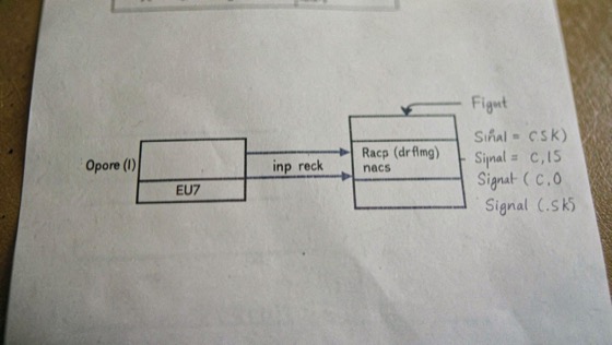
What the PIPE Interface Is, and What It Is Not
Link Basics
PIPE is the reason a controller core and a PHY from two different suppliers can be wired together at all. It is an interface specification, not a protocol layer.
-

Reading a training sequence in counts
Link Basics
The link training state machine is a fixed sequence, and the beginner who learns to count it can find the count a failing link never leaves.
-

The states that hold a link back
Link Basics
Between the working state and power off sit three pauses, and a device that is present but slow to answer is usually waking from one of them.
-
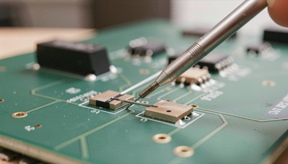
Link equalization in PCI express
Link Basics
Equalization becomes necessary above 5 GT/s because the channel stops behaving like a simple wire.
-
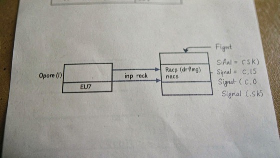
Ordered sets, DLLPs and TLPs on a PCIe link
Link Basics
A PCI Express link carries three distinct vocabularies at once: ordered sets, which are short fixed patterns used by the physical layer to keep the link aligned and trained; data link layer packets (DLLPs), which carry acknowledgements, flow control credits and power management handshakes between the two ends of a link; and transaction layer packets (TLPs), which carry the actual memory, I/O and configuration requests and completions.
-
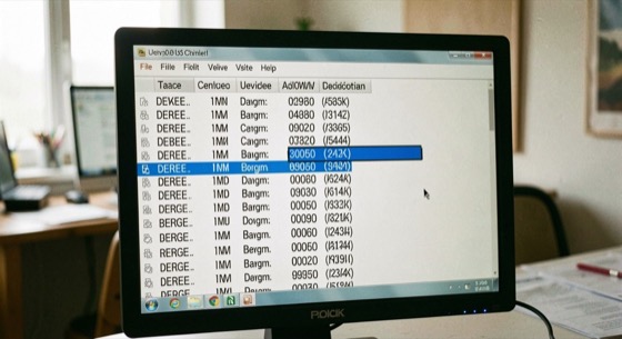
Reading PCIe capability registers
Link Basics
A capability register holds the encoded answer a PCI Express function gives when it is asked what it can do.
-
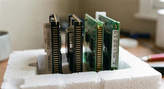
The Rate Ladder, Generation by Generation
Generations
Each generation of the base specification doubles the per lane transfer rate. The interesting part is what had to change underneath to make that doubling survive a real board.
-
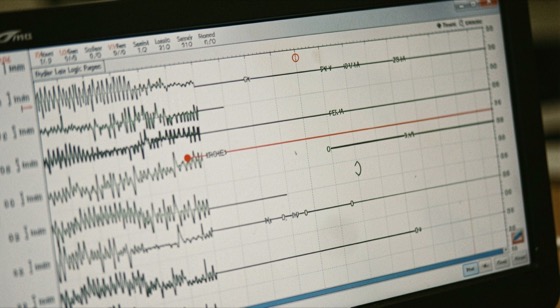
Encoding, Overhead and Usable Bandwidth
Generations
A transfer rate counts symbols on the wire. A byte rate counts what reaches the other side. The gap between the two is the encoding, and it changed once.
Four pages to begin with
The rules, the levels, the screening and the hunting day.
-
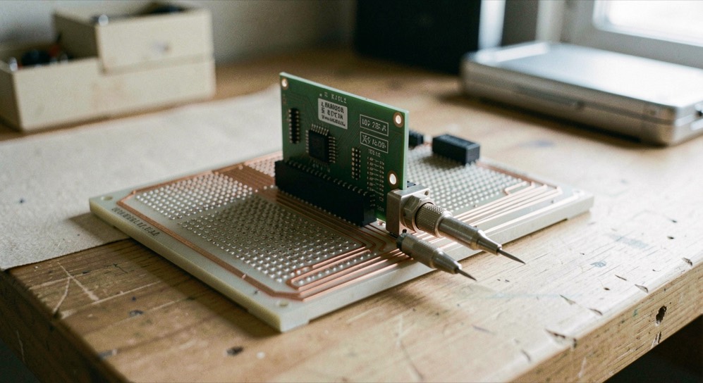
How a PCI Express Link Trains
Between power on and the first transaction, the two ends of a PCI Express link run a fixed sequence of states. Knowing that sequence is what turns a stuck link into a readable symptom.
September 6, 2026
-
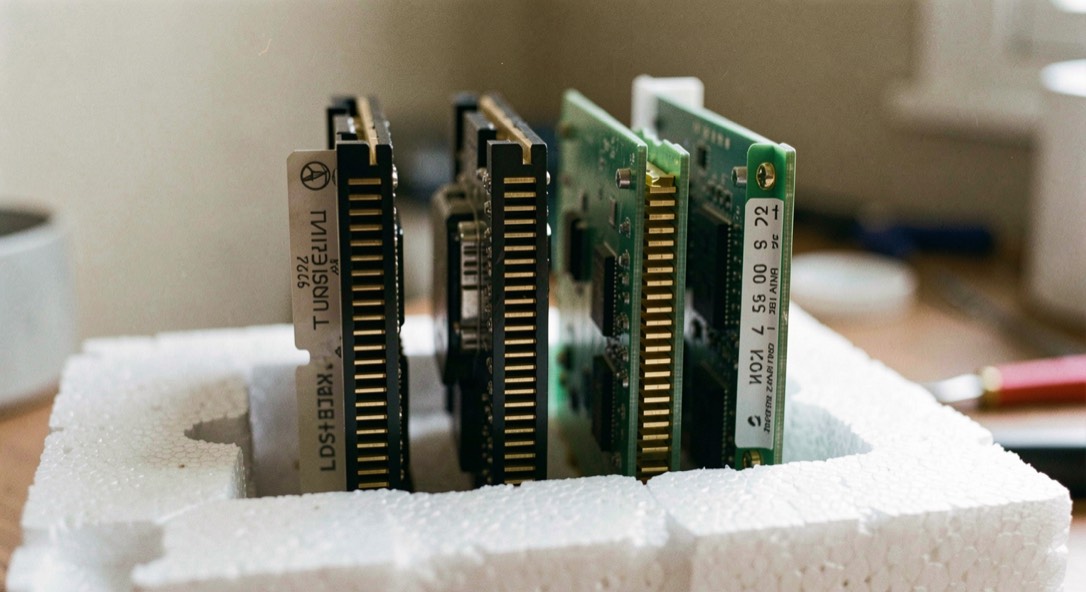
The Rate Ladder, Generation by Generation
Each generation of the base specification doubles the per lane transfer rate. The interesting part is what had to change underneath to make that doubling survive a real board.
September 6, 2026
-
The Solutions Catalog, Category by Category
This address used to hold a roster of catalog participants. The roster itself is gone and is not reconstructed here. Its structure survives in the archive, and the structure is the useful part.
September 5, 2026
-

Document 300312-001, and Where That Reading Goes Now
If you arrived from a chipset datasheet looking for document 300312-001, this page tells you what that reference was for and which current documents answer the same question.
September 5, 2026
This publication is not the PCI Special Interest Group, not a working group and not a chip vendor: it reads public specifications and vendor documentation and writes down what they say, which is set out on the about page. Every figure carries the document it came from and the day it was read, a procedure described in sources and method.
Read on other desks
Other desks reading public documents the way this one reads an interconnect, each on its own subject.
-
the LPFM rules
Generations
Citizens Radio Review reads the way this desk reads a specification: 100 watts, a thirty-meter antenna limit, channel protections and the point system, each figure traced to its filing.
-

commercial shipping decisions
Generations
Eitzen Group reads , tonnage, chartering, decarbonisation options and the rules that bind them, the way this desk reads an interconnect: by the document.
-

the XMPP standards process
Generations
Presence & Protocol reads Jabber and XMPP the way this desk reads interconnect specifications: from the published RFCs and extensions, with the history of how each document acquired its status, and is where its account begins.
-

a Tsim Sha Tsui stay
Generations
Tsim Sha Tsui Stay reads the way this desk reads a form factor: licensed guesthouses, the A21 bus into Nathan Road, budgets in HKD and twelve checks before a booking.
-

vinyl wrap film gauge
Generations
Another reading desk built on public specifications: The State Wraps Register keeps a dated spec table for , its chemistry, mil thickness, cut, adhesive and the weight it adds to the tube.
-

the tailings standard
Generations
A desk that reads a standard the way this one reads a specification: Thickened Ground Notes walks line by line for readers who are not engineers.
-
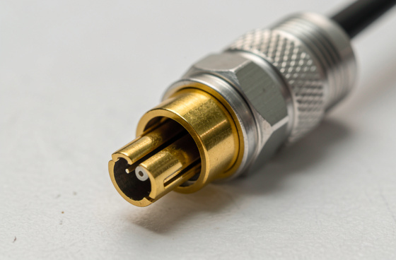
electroless nickel explained
Generations
The electroless nickel under a connector's gold flash has its own chemistry and its own failure modes; Hardface Notes keeps , with sources, for the reader who wants the deposit documented rather than sold.
-

a Mac's free space
Generations
Headroom reads the way this desk reads a link budget: the System Data category, purgeable space and local snapshots, measured before anything is deleted.